pcb board testing
Testing your printed circuit boards
We leave nothing to chance. To compete successfully in today’s global marketplace, you need to apply the right expertise at the right time to every stage of your product’s life cycle. That’s why MIS Electronics tests printed circuit board components and functionality with five different, powerful tests. Nothing passes unless it’s perfect.
GET A QUOTE
Our test services verify your product and test strategy. Get a no-obligation quote and get to market fast!
Automated Optical Inspection (AOI)
Components are getting smaller and circuits boards more complex. In AOI tests, a high-speed computer camera scans for missing components, positional divergence, wrong parts, lead defects reverses, solder integrity, and height variations to determine a pass or fail inspection:
- missing components, offset, incorrect parts, polarity
- Lifted leads, coplanar leads (<90° angle to board), tombstones (90° angle to board).
- Solder print (GERBER data, automatic sampling, or manual): solder paste, non-whetting, shorts, and lifted pins.
- Solder fillets (red LED light inspection with M22X fw): components that are missing, twisted or shifted, billboarded, upside down, or have the wrong polarity.
- Checks components down to 0603mm (0201″)


X-Ray testing
X-rays are high-resolution scans used on:
- BGAs
- Micro BGAs
- Chip scale packages
- Large boards
What kind of faults are discovered with x-ray tests?
Opens
OPENS
Opens are usually caused by insufficient reflow, missing balls, doming, popcorning, or contaminated board surface conditions.
Shorts
SHORTS
A short circuit is a connection that was not meant to be there.
Insufficient reflow
INSUFFICIENT REFLOW
More difficult to spot. A solder joint with an irregular shape and a rough, grainy appearance at the edges.
Doming
DOMING
A defect from improper storage (not in nitrogen or other non-humidity chambers). The centre solder joints of the BGA are slightly smaller than those on the outside edge.
Potato chipping
POTATO CHIPPING
An overheated component's outside edge lifts up from a pad, making the centre joints look squashed.
Voids
VOIDS
Happen on boards without a long-enough reflow. Created by flux gases that are unable to escape.
In-circuit tests (ICT)
An electrical probe is used to check a PCB for shorts, opens, resistance, and capacitance to check whether the assembly was correctly fabricated. An In-Circuit test detect manufacturing process faults quickly and accurately .M.I.S. Electronics offers in-circuit test and turnkey test program development and fixture fabrication services.

Standard PCB program development
The Standard programs are cost-effective and offer a fast turn-around. This service is most suitable for customers with standard technologies or limited time and budget. The Standard programs can be upgraded to an Advance level at a later date if required.
Advanced test program
Designed for complex boards and for customers that require the maximum fault coverage possible at the ICT stage, the advanced programs adds these steps onto the standard program:
Combo PCB ICT & Functional Test Programs
COMBO ICT + FUNCTIONAL
Although ICTs detect faults quickly and accurately, they aren't functional. As such, MIS Electronics expands on the ICT by integrating off-the-shelf instruments (GPIB, VXI or PXI) and the necessary electronics to design, build, and debug a test fixture to test functionality. The fixture is integrated with the ICT system software before it's installed at the customer’s site.
Single-stage PCB test strategy
SINGLE-STAGE PCB TEST STRATEGY
A logical approach combines In-Circuit Testing (ICT) and Functional Testing (FBT) into a single-stage, when possible, to achieve higher fault coverage that may not be possible with ICT-only tests. A single test fixture saves test time and capital expenditure, reducing the potential for errors and damage caused by excessive board handling.
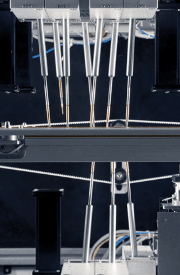
Flying Probe test
Fast, accurate, high-fault coverage.
A flying probe is an electro-mechanical controlled probe that accesses components on a PCB assembly accurately and quickly. Flying Probe pcb testing provides high fault coverage with repeatability—there’s no need for a test fixture.
Probe precession can access various assembled components such as PLCCs, SOICs, PGAs, SSOPs, and QFPs on PCB assemblies.
PCB Flying Probe Tests are ideal for
- PCB Production ramp-up
- PCB Prototype test
- PCB Sample board test
- Large boards

JTAG Boundary scan test & on-board device programming services
Using powerful PCB boundary scan hardware and software products (ScanMaster & ScanManager), we support the following applications:
- Flash programming
- ISP programming
- Structural test
- Cluster functional test
- Memory test
Circuit board assembly is one piece of the turnkey puzzle.
Trust MIS Electronics to manage your product from custom design to delivery,
ensuring a retail-ready board without errors.
We’re well established in the key areas of on-time delivery, cost control,
fast prototyping, highest quality and total care support.
ensuring a retail-ready board without errors.
fast prototyping, highest quality and total care support.
Our Office
MIS Electronics Inc.
174 West Beaver Creek Rd.
Richmond Hill, ON L4B 1B4 Canada
ISO 9001:2015 registered
ISO 13485:2016 registered
Office Hours
Mon-Fri: 9am - 5pm (EST)
Sat-Sun: Closed
Electronics careers
Certifications
Our Office
MIS Electronics Inc.
174 West Beaver Creek Rd.
Richmond Hill, ON L4B 1B4 Canada
ISO 9001:2015 registered
ISO 13485:2016 registered
Office Hours
Mon-Fri: 9am - 5pm (EST)
Sat-Sun: Closed
Contact Us
1 905-707-2305