
An electronics chip used to be an out-of-reach commodity accessible only by deep-pocket companies with large print-run requirements. But today’s printed circuit board (PCB) designs can be professionally-made for anyone who has a prototyping and production need.
With a little professional guidance, you can design and customize a PCB to fit any project.
Want to learn how to create a high-quality PCB layout design? Here is a complete guide with everything you need to know!
The Basics of PCB Layout Design
Start by asking these questions to figure out what you need:
- How big does your PCB need to be?
- Will it end up in a giant piece of medical equipment, a handheld device, or possibly a hearing aid?
- how fast does it need to be?
- How smart will it be?
- How durable?
Everything about your design stems from the PCB’s ultimate use. Here is a handy PCB design flow chart put out by the Institute for Printed Circuits (IPC) you can use as a reference guide for PCB design and production standards. But this is a complete guide, so we’ll dive a little deeper.
If you understand the significant parts of a PCB, if you know what to consider when planning your project, and if you have the right resources, you can design the PCB of your dreams.
So let’s get started!
The Substrate
PCB components rest on a solid foundation known as a substrate. Typically a type of fiberglass, like F4, the substrate is very durable and can range in thickness from .8mm to 1.6mm.
FR4’s main advantages are that it can withstand high levels of stress and heat.
Keep in mind that the substrate thickness can affect the amount of impedance (electrical resistance) throughout the board. Also, drill holes that penetrate through the entire board can mess with a thinner board’s integrity, causing it to warp and the components to shift.
Keep in mind that thinner circuit boards tend to break if they get too big, which is one reason you may opt for a thicker substrate when creating your custom PCB.
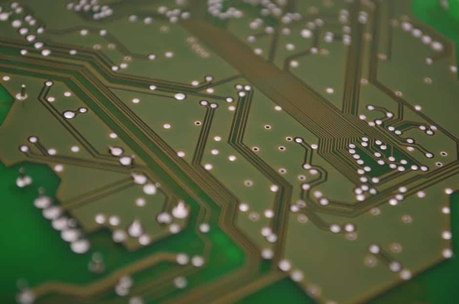
Copper Tracings
Next comes the essential copper layer.
Back in the day, circuit boards were huge and filled with wires because they relied on point-to-point communication between components. Fast forward a few generations, and you get a quantum leap of efficiency in the form of copper traces. Copper traces are micrometre-thin “trails” of copper that act as wires once did, integrating all of the PCB’s components.
Copper traces start as a single, flat layer. Then, an intricate chemical process burns off everything that will not serve as a trace, leaving only a network of copper trails: the PCB’s nervous system.
You can choose to design your PCB with a copper layer on one side, both sides or make it multilayered. As you might imagine, the more functionality your PCB demands, the more layers of copper tracings it will need. Copper is the darling conductor of electronics, and part of this means generating heat; the more copper layers in your PCB, the hotter it will get. Also, more layers (and thicker substrate) will translate to a higher manufacturing cost.
One of the hallmarks of good PCB designs is efficiency. At MIS. Electronics, we ensure you purchase only the PCB your project needs. Whether you’re prototyping or you’re ready to scale, we respect your bottom line and keep your project cost-effective.
The Soldermask and Silkscreen
The soldermask is the next outer layer of the circuit board. The soldermask covers the network of copper trails to protect, or “mask,” it from the effects of soldering. You may have to attach or remove components from your PCB, and the last thing you want is for your solder gun to make contact with the copper trails. Hot wiring your copper trails can spell disaster for your entire PCB! The soldermask is also where you get the PCB’s distinct colors: typically red, blue, green, or black.
The silkscreen is the final, most superficial layer. Important symbols and the PCB’s brand logo go on the silkscreen.
PCB Components
Finally, the PCB components (all the little pieces that make your circuit board work) are assembled. From capacitors to resistors, the amount of functionality packed into these tiny devices is endless!
While there is too much detail to go into here, some of the most common PCB components include:
- Diodes
- Transistors
- Resistors
- Switches
- Relays
- Integrated Circuits
The best part of customizing your PCB is that you can finetune it to fit your needs. If you are an independent inventor or an engineer for a small R&D department, use MIS electronics to source the highest quality components for a perfect PCB.
Design Software and Files
There are several computer-aided design (CAD) programs made especially for PCB layout. Some PCB software programs cost a pretty penny, but some are free.
With the right software program, you’ll lay out all aspects of your PCB, including:
- Circuit design
- Component placement and orientation
- Drill hole placement
- Logo and design placement
Your initial software design yields different files for all aspects of your PCB design.
The Bill of Materials (BOM) is the complete list of parts included for your circuit board, and one of the most important files when it comes to estimating the real cost of production for your PCB.
The Gerber files include all of the information about your PCB’s layers. From the copper to the substrate thicknesses, Gerber files are a critical piece of information for PCB manufacturing. You can also use OCB ++ files in the place of Gerbers.
Centroid files, or “XY” files, list the coordinates and orientation for all of the surface-mounted electrical components.
Finally, the net files outline the connections within the circuit.
The Professionals by Your Side
All of this information helps the manufacturer understand the viability of your PCB layout design. But don’t think you have to go it alone. If you have an idea, engage with experts to step through the stages of PCB design. As one of the largest PCB manufacturers in North America, our friendly engineers will take your PCB from design to final product in the shortest amount of time, using the fewest, most cost-effective parts, assembled the most efficient way. We turn your concept into a high-quality product that hits shelves in record-time.
Contact our team today to see how we can help make your PCB concept a reality.