

Imagine starting the day with a broken smartphone—the very idea is painful, isn’t it?
In today’s techno-centric era, it’s easy for manufacturers to create new gadgets. But it’s easier to make them mediocre than it is to make them top tier. What’s the difference between a great gadget and one that’s glitchy? High-quality components in electronics, intelligent design, best practices in manufacturing, and meticulous testing are all important for successful electronics. These things add pennies and seconds to the race. Some opt to tighten the straps on budget and loosen the reins on speed. But cheaper and faster is a recipe for junk. Shortcuts don’t make long delays in electronics. They make broken toys.
Cheap electronic toys and gadgets manufactured in low-cost destinations, without methodical testing procedures and quality control are prone to failure. Interestingly, sometimes gadgets fail not because of defective components, but because of bad design, insufficient product testing, and a lack of understanding of the target users.
Famously glitchy gadgets
From tech giants like Google, Facebook, and Amazon, to newly built companies and start-ups, everybody has a shame story to tell. The world of business follows Murphy’s law:
“Anything that can go wrong will go wrong.”
The list of companies that fail to understand this basic concept grows every year. More than 90% of start-ups fail in the first 10 years. A large portion of these failures are not due to the wrong idea; they are due to incorrect execution and a lack of testing the market.
A case in point for failure due to a lack of testing is the original iMac Mouse.
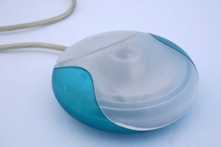
Released with the first iMac, it received good press for its elegant look. But soon, reports came in that it was uncomfortable for long use and led to hand cramps. Ultimately, Apple had to replace it with a more traditional mouse design.
It is common for entrepreneurs and businesses to be overly optimistic about the new products they launch. There’s a certain energy that surges off the start. But to succeed, every product must face a reality check. Numbers speak the truth, not theories (or hopes).
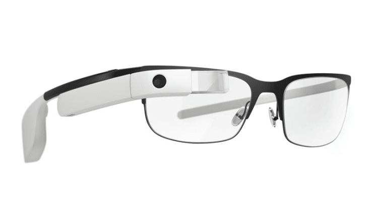
Google Glass is an example of a product that failed because no one wanted it! The product designers were not clear about its use cases. It was a product that held no meaningful benefits for its users and it failed to succeed in the market. It didn’t even look cool. The company failed to test the prototype in real-life scenarios and modify the design according to user feedback.
PCB design for great gadgets: Some challenges
At the heart of any electronic gadget is the printed board circuit or PCB. It is the most critical component of today’s electronic and industrial world.
For a product to be successful in the market, the PCB at its core must be well-designed and manufactured. Just as complex electronics components resistors, capacitors, transistors, diodes, and fuses can have defects, so can PCBs.
PCB manufacturers face many challenges during the design phase. Let’s look at some:
1. Burnt Components:
In compact PCBs, if the space around components is insufficient, the temperature rises. These high temperatures burn the surrounding components. Depending upon the size, structure, and material of the component, it can absorb only up to a certain amount of heat. These parameters must be addressed during the design phase.
2. Pad Lifts:
The solder pads sometimes shear off from the PCB trace due to excessive heat or pressure on an existing joint. These are difficult to repair as their position lies in the blind spot region of the technicians.
3. Blowholes and Pinholes:
As the names suggest, these appear as holes in the solder joints in larger and smaller sizes respectively. These holes are generally created during the wave soldering process due to moisture in the boards. Such circuits fail to conduct as expected for a long duration.
4. Environmental Factors:
Multiple environmental factors such as temperature, moisture, and dust, pose different challenges. Temperature fluctuations cause PCBs to malfunction as they damage the soldering joints. Moisture adds holes and causes corrosion, oxidation, and rusting in the PCB. Dirt can clog the equipment and also cause over-heating.
5. Insufficient Wetting:
This issue is found both at joints as well as SMD components. In the case of joints, it occurs due to an uneven supply of heat to the pin and the pad, or due to insufficient time provided to the solder to flow. In the case of SMD components, it is usually responsible for missed soldering failure leading to falling off of components.
There is no foolproof method to completely prevent such challenges. Of course, companies cannot avoid failure altogether. But those that adopt best practices in the design and manufacturing process reduce the incidence of PCB failures.
Manufacturers must perform a detailed PCB failure analysis to prevent defects and improve their product’s quality. Once they identify the root cause of the failure, they can correct the fault and prevent it from recurring.
PCB failure analysis techniques
There are several techniques available to identify PCB defects, including electrical testing, visual inspection, radiography, X-ray fluorescence, and acoustic microscopy.
PCB failure analysis techniques help in eliminating different factors that can potentially cause failure instead of looking for signs of failure after it occurs. This includes every little detail ranging from highlighting the presence of contaminants on the board to minute cracks on the board.
Unlike traditional surface analysis, PCB failure analysis employs multiple advanced failure analysis techniques.
1. Solderability Testing:
This test reduces the chances of failure during the PCB manufacturing process. It tests the solderability of the pad to make sure the surface is robust. This increases the chances of forming a strong joint.
2. PCB Contamination Testing:
In this test, the PCB sample is immersed in a solution which quantifies the contamination using the ionic technique. If the readings are within industry standards, the PCB is accepted. This test is highly accurate and precise.
3. X-ray Inspection:
This test identifies internal as well as surface flaws. It is also used to test components with hidden joints and parts located underneath a chip. This is a non-destructive technique (NDT) and maintains the sample in pre-testing condition. Other NDT techniques include electrical characterization, acoustic microscopy, and thermal imaging.
4. Design Testing:
Design testing ensures that the product’s physical design is strong enough to withstand usage and environmental stresses, has an appealing look, and is easy to use.
MIS: The secret ingredient in great gadgets!
Electronics manufacturers have a lot to gain from leaning on high-quality PCB manufacturers. Ultimately, PCB design, manufacturing, and testing excellence play a big part in ensuring their gadgets turn out great – not glitchy!
Turn to MIS for services throughout the PCB lifecycle. From concept to delivery, we provide high-quality PCBs, prototyping, advanced electronics assembly solutions, and superior testing services, with fully supported turnkey solutions.
MIS proudly operates from Canada. North American electronics PCB manufacturers are known for higher quality components, rigorous testing and inspection, and customer service that focusses on long-term customer care.
With MIS, you’re assured of faster time-to-market, fewer uncertainties, complete end-to-end support, and lower bottom line costs than working with an offshore manufacturer.